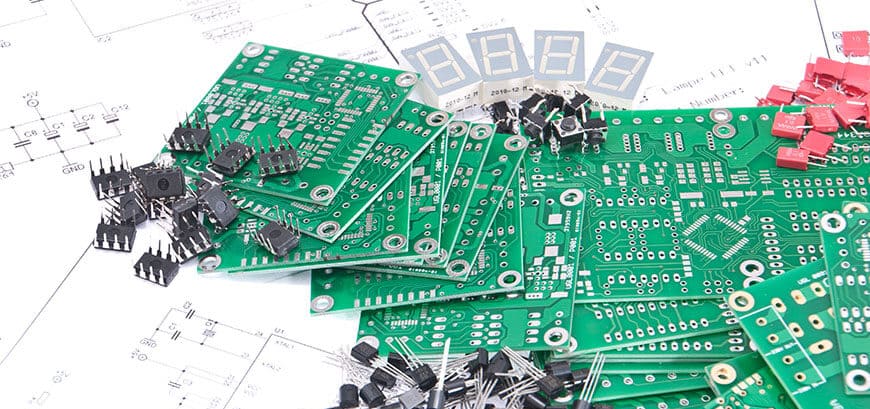
Basic Introduction to PCB Assembly
In the modern electronics field, PCB assembly is undoubtedly the core link in building all kinds of electronic products. It is like the “foundation” of electronic products, directly determining the performance, quality and success of the equipment. Whether it is a smartphone that leads the trend of technology, a sophisticated wearable technology device, or a mechanical control unit that plays an important role in the industrial field, PCB assembly plays a vital role.
However, PCB assembly is not a simple patchwork of parts. It involves complex technology, strict processes and meticulous quality control. So, what is the process of PCB assembly? Why does it play such a pivotal role in electronic manufacturing? This guide will take you to explore the mysteries of PCB assembly and fully present the essence of this critical process.
1.Detailed explanation of PCB assembly process
The following is a detailed PCB assembly process:
1.PCB Design and Preparation
Design Phase
Engineers use design software (such as Altium, Eagle or KiCad) to create PCB layout, including details such as component location, board size, electrical connection routing, etc.
File Conversion
After the design is completed, it is converted into a Gerber file, which serves as a blueprint for manufacturers to manufacture the physical PCB, including all key information such as layers, component placement and electrical routing.
2.Bare board PCB manufacturing
Production process
Manufacturing bare PCBs, usually made of layers of fiberglass, copper, and insulating materials. First, the copper layer is etched to create electrical pathways, and then holes are drilled for through-hole components and vias (inter-layer connections). After that, the board is cleaned and coated with solder mask to protect the copper wires and ensure the correct soldering position.
3.Component procurement and preparation
Procurement phase
Order electronic components that meet the design specifications from different suppliers, including miniature resistors, capacitors, complex ICs, etc.
Preparation work
Ensure that the components meet the requirements in terms of size, power rating, and function, and prepare for assembly.
4.Component placement
SMT component placement
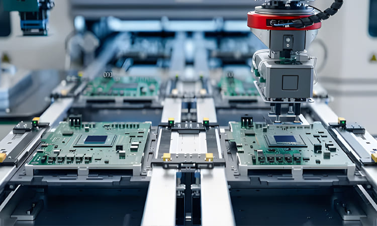
For SMT, a pick-and-place machine is used to accurately place components on pads on the PCB that have been coated with solder paste. Solder paste is a mixture of solder balls and flux, and the accuracy of coating is ensured by a template.
5.Reflow soldering
Soldering principle and process
The PCB enters the reflow oven and is heated in stages to melt the solder paste, which forms a firm connection between the component and the circuit board after cooling. This process needs to be strictly controlled to prevent component movement and defects such as solder bridges and cold soldering.
6.Through-hole component assembly
Insert and soldering
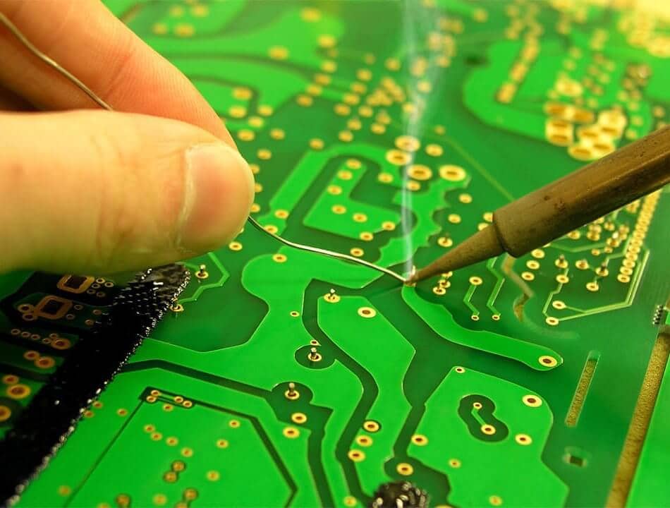
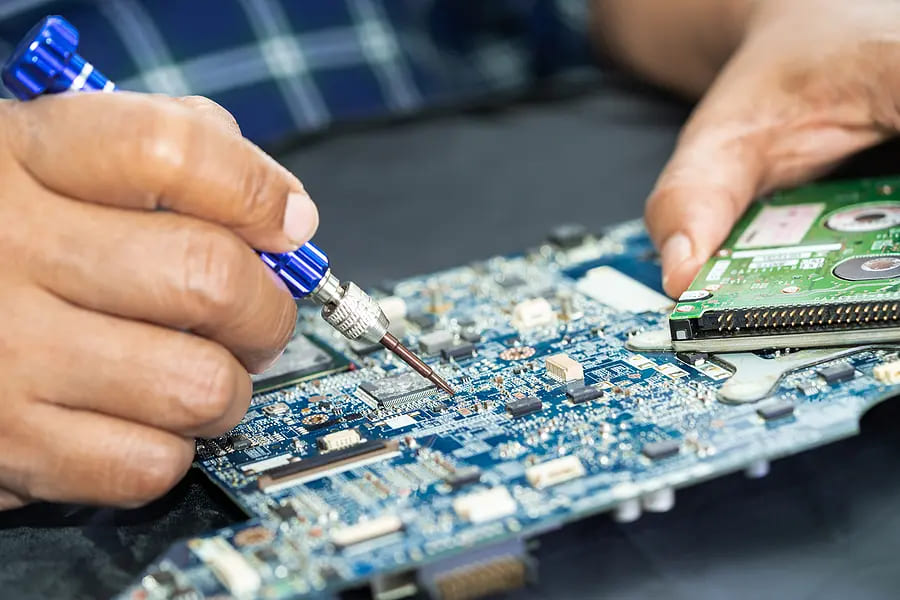
If THT is used, the leaded component is inserted into the PCB drilled hole and then soldered manually or by a wave soldering machine. During wave soldering, the bottom of the circuit board is exposed to the molten solder wave, causing the solder to adhere to the leads and pads.
7. Inspection and quality control
Inspection methods
Automated optical inspection (AOI) is used to scan the PCB to check for visual defects; for complex circuit boards, such as those containing BGA, X-ray inspection is used to verify the integrity of hidden solder joint connections; manual visual inspection is also performed in some cases, especially for small batch production.
8.Functional testing
Test types
Includes in-circuit testing (ICT) to test each component on the circuit board, and functional testing to power up the entire circuit board to ensure that it can perform the required functions, such as signal processing or communication with other components.
2.Common PCB assembly technology
Surface mount technology (SMT)
Technical principle
SMT is the mainstream method of modern PCB assembly. It places tiny surface mount devices (SMDs) directly on the surface of the PCB and connects them to the pads through welding.
Advantages
Compact and lightweight: It can accommodate smaller components, making electronic products such as smartphones lighter and thinner;
Fast assembly speed: Highly automated machines can mount thousands of components per hour, suitable for mass production
Economic and efficient: Due to automation and component miniaturization, the cost is relatively low, especially in mass production;
High performance: Suitable for high-frequency circuits, because smaller components generate less interference, it is ideal for advanced devices.
Application
Widely used in consumer electronics (such as smartphones, laptops, tablets), telecommunications equipment, industrial control systems, and automotive electronics (such as automotive infotainment systems).
Through-hole technology (THT)
Principle
THT is a traditional PCB assembly technology. The leads of through-hole components pass through the drilled holes on the PCB and are soldered to the pads on the other side to form a solid connection.
Advantages
Stronger connection: Suitable for heavy industrial equipment and aerospace electronic equipment, which require high ruggedness and durability
Adapt to large components: such as connectors, transformers, and large capacitors
Convenient manual assembly: For small batch production, it is convenient for manual assembly because larger components are easier to operate.
Hybrid technology
Technical principles and advantages
Hybrid technology combines the advantages of SMT and THT, using both technologies on the same circuit board. It has the flexibility to obtain the advantages of space saving and high performance of SMT, and the strength or size advantages of THT components. It is suitable for complex designed products, such as equipment that requires both small high-speed components and larger durable components.
Application scenarios
Widely used in automotive systems (such as a mix of sensors, controllers and heavy components), medical equipment, high-end communication systems, and IoT devices.
3.Common Problems of PCB Assembly
1.Component misalignment
Problem cause
The components may not be accurately placed on the PCB due to problems with the placement machine, improper solder paste application, or poor circuit board design, which may cause serious functional problems or even circuit board failure.
Solution
Fine-tune the placement machine to ensure correct calibration, check mechanical problems and adjust the speed; check the solder paste template to ensure even application, use high-quality templates and clean them regularly; improve PCB design, follow the design for manufacturing (DFM) principles, ensure that the pad design has sufficient tolerance, and use reference marks to assist component alignment.
2.Solder bridging
Problem cause
Excessive solder forms unexpected connections between pads, usually caused by excessive solder paste or incorrect reflow oven settings, which may cause circuit board short circuits.
Solution
Optimize the amount of solder paste and adjust the template aperture to ensure the right amount; check the reflow temperature curve and fine-tune the temperature according to the component and solder type; check the pads and layout, and appropriately increase the pad spacing or adjust the pad size. Use the AOI system to detect solder bridge problems in a timely manner.
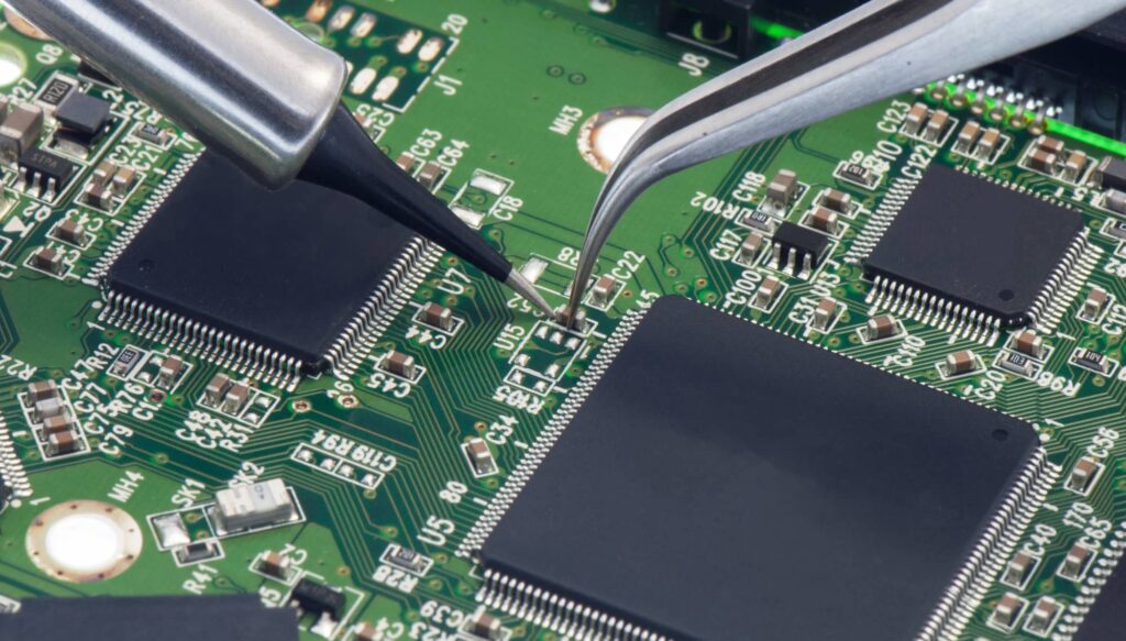
3.Tombstoning effect
Problem cause
During the reflow process, one side of the component is lifted from the pad, like a tombstone, mostly due to uneven heating or different surface tension of the solder on the pad, which is common in the SMT process.
Solution
Balance reflow heating to ensure that the reflow oven heats the circuit board evenly; use the appropriate pad size to ensure uniformity and according to the component design; optimize the solder paste application to ensure that both sides of the component are evenly coated. Consider switching to smaller, lighter components with uniform heating characteristics to reduce risks.
4.Solder voids
Problem cause
Air pockets trapped in the solder joint weaken the connection, affecting electrical performance and reliability, usually caused by improper reflow curve or solder paste contamination.
Solution
Adjust the reflow curve and heat slowly to allow air to escape; use high-quality solder paste, ensure it is fresh and store it properly to avoid moisture or oxidation; for critical applications, a vacuum reflow oven can be used to reduce the occurrence of voids. Use X-ray inspection to detect voids, especially when dealing with hidden components such as BGA.
5. Production delay
Causes
It may be caused by a variety of reasons such as shortage of parts and rework of defective circuit boards, which will affect production schedule and cost.
Solutions
Strengthen supply chain management, pay attention to inventory and delivery time, cooperate with reliable suppliers and maintain buffer inventory; use DFM guidelines to optimize PCB design, reduce errors and rework time; realize automated production and quality inspection as much as possible, such as using AOI or X-ray inspection, etc. Conduct trial production to find problems in advance and avoid subsequent troubles.
Summary
PCB assembly, as the core process of electronic manufacturing, covers a variety of key technologies, complex process steps and fine quality control points. Understanding different assembly technologies and their applicable scenarios, mastering detailed assembly processes, and effectively responding to common assembly challenges are essential to ensure the quality and efficiency of PCB assembly.
With the continuous development of electronic technology, PCB assembly technology is also evolving continuously, and trends such as automation and intelligence will further promote the improvement and innovation of this process. By continuously optimizing technology and processes and solving problems in actual production, we can achieve higher quality and more efficient PCB assembly. Whether it is a professional electronic engineer or an industry practitioner, a deep understanding and mastery of PCB assembly technology will lay a solid foundation for their innovation and development in the electronics field.
