Semiconductor equipment parts: manufacturing and processing of machine parts
In the process of semiconductor parts manufacturing, although the core chip part is manufactured through semiconductor processes such as lithography, etching, deposition, etc.
But there are still many structural parts, packaging parts and semiconductor equipment parts that need to be machined to complete. The following are the main semiconductor components and semiconductor equipment parts manufactured by machine processing, and their uses, processing methods, typical materials and precautions are listed in detail.
1.Semiconductor equipment parts: equipment structural parts
These parts are mainly used in semiconductor manufacturing equipment, such as etcher, lithography machine, ion implanter, etc.
(1) Chamber
Use: vacuum chamber used for manufacturing processes such as plasma etching, CVD, PVD, etc.
Processing method: CNC milling, CNC turning, precision grinding.
Typical materials: aluminum alloy (6061, 7075), stainless steel (316L), ceramic, titanium alloy.
Precautions: Aluminum alloy chambers are usually milled by high-speed CNC to reduce the heat affected area and improve the surface finish. Stainless steel chambers require low-speed cutting and sufficient cooling to prevent work hardening.
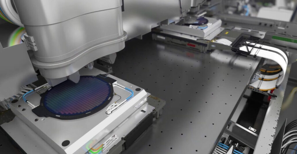
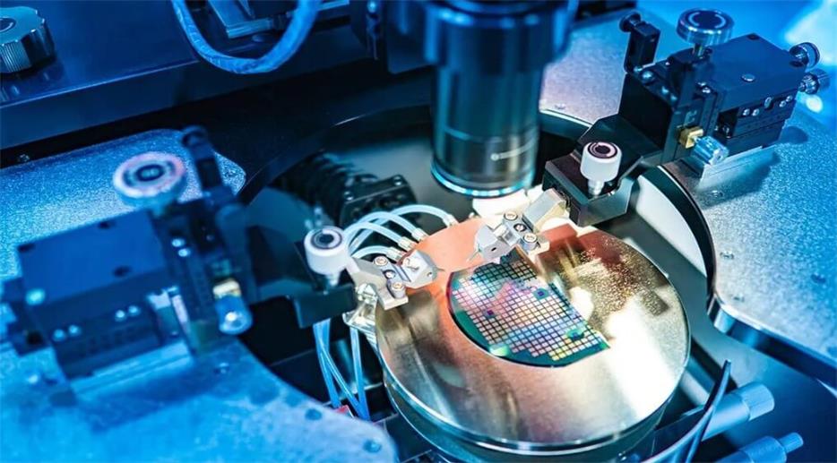
(2) Wafer Carrier/Holder
Purpose: Fix the wafer (silicon wafer) to prevent the wafer from moving during processing.
Processing method: CNC precision milling, drilling, grinding.
Typical materials: quartz, alumina ceramics, PEEK (polyetheretherketone), stainless steel.
Notes: CNC precision milling the surface of the carrier to ensure flatness and reduce the risk of wafer breakage. Ultra-hard alloy tools must be used for drilling small holes, and the feed rate must be controlled to prevent material cracking.
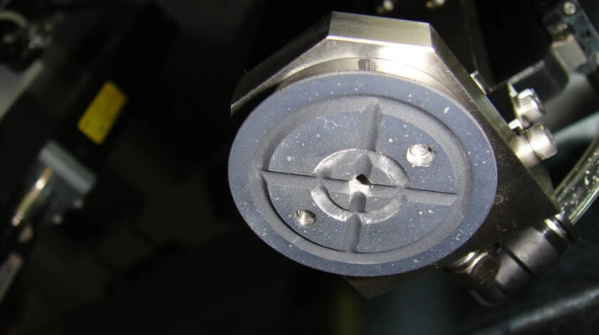
(3) Vacuum Chuck
Purpose: Used to fix wafers in photolithography machines or etching equipment.
Processing method: CNC precision milling, CNC micro-drilling (manufacturing microchannels).
Typical materials: ceramics, aluminum alloys, silicon carbide (SiC).
Notes: Micro-drilling uses laser or ultrasonic processing to ensure aperture accuracy. Aluminum alloy materials are finely processed using high-gloss tools to reduce surface roughness.
(4) Heater Chuck
Purpose: To heat the wafer during photolithography or etching to ensure uniform temperature distribution.
Processing methods: CNC milling, grinding, drilling (for embedding heating elements).
Typical materials: quartz, ceramics, graphite, aluminum alloy.
Notes: Aluminum alloy heat chucks are processed using high-precision CNC milling to ensure surface flatness. Graphite materials must be processed at low speeds and a vacuum system must be used to reduce the impact of dust.
2.Sensor and packaging components
Mechanical parts used for semiconductor devices or final sensor products.
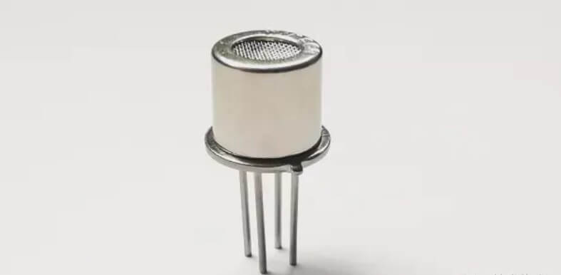
(1) Metal Package
Purpose: Used for packaging of gas sensors, pressure sensors, photoelectric sensors, etc.
Processing methods: CNC turning, CNC milling, laser welding.
Typical materials: Kovar alloy, stainless steel, aluminum alloy, titanium alloy.
Note: When CNC turning Kovar alloy, low-speed cutting is required to prevent deformation during processing. The shell sealing surface needs to be precisely milled to ensure the fit of subsequent welding.
(2) Ceramic Package Base
Purpose: Used for packaging of high-end power devices and optical communication devices.
Processing method: Precision milling, grinding, laser cutting.
Typical materials: Alumina ceramic (Al₂O₃), aluminum nitride (AlN).
Typical materials: Diamond tools must be used when machining ceramic materials to prevent edge collapse. After precision grinding, ensure the flatness and finish of the package base.
(3) Heatsink
Purpose: Used for heat dissipation of power semiconductor devices (such as IGBT modules, LED chips).
Processing method: CNC milling, CNC turning, broaching, drilling.
Typical materials: Copper, aluminum alloy, composite materials (such as graphene-coated copper).
Note: Aluminum alloy heat sinks use high-speed milling to speed up production efficiency. When processing copper materials, the amount of cutting fluid must be controlled to prevent copper chips from sticking to the tool.
3.Semiconductor equipment parts: precision alignment and handling components
Motion systems or precision alignment systems used for semiconductor manufacturing equipment.
(1) Alignment stage
Purpose: High-precision alignment system for photolithography machines and etching machines.
Processing method: CNC high-precision milling, grinding, wire cutting.
Typical materials: ceramics, stainless steel, titanium alloy.
Note: Use high-precision CNC milling to ensure the parallelism of the guide rails and reduce motion errors.
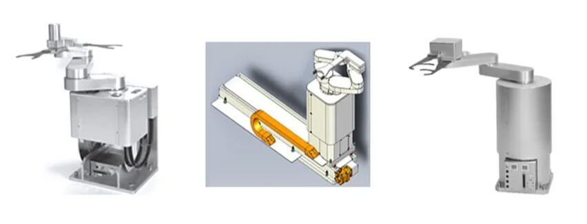
(2) Wafer handling robot arm
Purpose: Used in automated production lines to transport silicon wafers.
Processing method: Turning, milling, precision welding.
Typical materials: carbon fiber, aluminum alloy, titanium alloy.
Note: Carbon fiber parts need to be processed with special tools to reduce the risk of delamination.
(3) Optical Mount
Application: used for semiconductor testing equipment such as laser alignment and optical measurement.
Processing method: CNC milling, CNC micro-drilling, surface grinding.
Typical materials: titanium alloy, alumina ceramic, stainless steel.
Notes: High-precision drilling combined with laser cutting to ensure the installation accuracy of optical components.
4.Chemical treatment and fluid control components
Used for chemical treatment in processes such as etching, deposition, and chemical mechanical polishing (CMP).
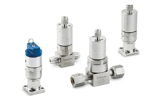
(1) Fluid Control Valve
Application: control the flow of chemical gases and liquids.
Processing method: CNC turning, milling, precision polishing.
Typical materials: PFA (perfluoroalkoxy resin), PTFE (polytetrafluoroethylene), stainless steel.
Notes: CNC precision turning the inner cavity of the valve body to reduce fluid resistance and improve sealing.
(2) Gas Distribution Plate
Purpose: Used for uniform gas distribution in processes such as plasma etching and CVD.
Processing methods: CNC micro-drilling, CNC milling, sandblasting.
Typical materials: quartz, ceramic, stainless steel.
Notes: Micro-drilling uses electrospark machining to ensure uniform gas flow distribution.
5.Other semiconductor equipment parts
Auxiliary parts for various semiconductor manufacturing and testing equipment.
(1) Test fixture
Purpose: Used for electrical testing and functional testing of semiconductor devices.
Processing methods: CNC milling, CNC drilling, tapping.
Typical materials: PEEK, aluminum alloy, stainless steel.
Notes: CNC milling ensures precise positioning and reduces the impact of errors.
(2) EMI Shield
Purpose: Used for semiconductor packaging to prevent electromagnetic interference (EMI).
Processing methods: stamping, laser cutting, bending and forming.
Typical materials: nickel alloy, stainless steel, aluminum alloy.
Note: Use laser cutting and bending to ensure electromagnetic shielding effect.
6.Summary
To sum up, although machining technology is not directly used in chip manufacturing, it is crucial in the entire semiconductor production chain. It is mainly used to produce semiconductor structural parts and semiconductor equipment parts.